3
FN6830.0
December 19, 2008
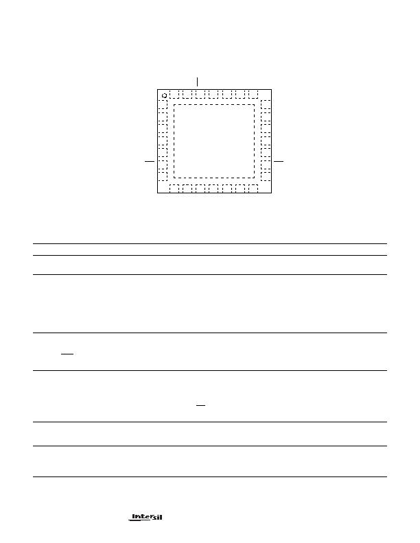
Pinout
28 LEAD QFN
TOP VIEW
1
2
3
4
5
6
7
21
20
19
18
17
16
15
28 27 26 25 24 23 22
8
9 10 11 12 13 14
SNS2
VO2
SS2
GT2
FLT2
PG2
TCB2
SNS1
VO1
SS1
GT1
FLT1
PG1
TCB1
Pin Descriptions
PIN
NAME
FUNCTION
DESCRIPTION
1
SNS1
Current Sense Input
This pin is connected to the current sense resistor and control MOSFET Drain node. It provides
current sense signal to the internal comparator in conjunction with VS1 pin.
2
VO1
Output Voltage 1
This pin is connected to the control MOSFET switch source, which connects to a load. Internally, this
voltage is used for SS control.
3
SS1
Soft-Start Duration Set
Input
A capacitor from this pin to ground sets the output soft-start ramp slope. This capacitor is charged by
the internal 10礎 current source setting the soft-start ramp. The output voltage ramp tracks the SS
ramp by controlled enhancement of FET gate. Once ramp-up is completed, the capacitor continues
to charge to the CPVDD voltage rail. If common capacitor is used (by tying SS1, SS2 together and
the capacitor to GND from the connection) then both the outputs track each other as they ramp up.
4
GT1
Gate Drive Output
Direct connection to the gate of the external N-Channel MOSFET. At turn-on the Gate will charge to
4 X Vbias or 10V(max) from the 24礎 source.
5
FLT1
Fault Output
This is an open drain output. It asserts (pulls low) once the circuit breaker delay (determined by the
TCB timeout cap) has expired. This output is valid for Vbias>1V.
6
PG1
Power Good Output
This is an active low, open drain output. When asserted (logic zero), it indicates that the voltage on
UV1 pin is more than 643mV (633mV + 10mV hysteresis). This output is valid at VBIAS >1V.
7
TCB1
Circuit Breaker Delay
Timer
A capacitor from this pin to ground sets the delay from the onset of an over current event to channel
shutdown (circuit breaker delay). Once the voltage on TCB cap reaches V
CT_Vth
the GATE output is
pulled down and the FLT
is asserted.
The time for circuit breaker delay (t
CB
) = (C
TCB
*1.178)/10礎.
8
DNC
Do not connect
Do not connect
9
GND
Chip Gnd
This pin is also internally shorted to the metal tab at the bottom of the IC.
10
PGND
Charge pump ground. Both GND and PGND must be tied together externally.
11
CPQ-
Charge Pump Capacitor
Low Side
Flying cap lowside.
ISL6174
发布紧急采购,3分钟左右您将得到回复。
相关PDF资料
ISL61861DCBZ
IC USB PWR CTRLR 3A 8SOIC
ISL6402IR
IC REG TRPL BCK/LINEAR 28-QFN
ISL6413IRZ-TK
IC REG TRPL BCK/LINEAR 24-QFN
ISL6432CB-T
IC REG QD BCK/LINEAR 16-SOIC
ISL6521CBZS2698
IC REG QD BCK/LINEAR 16-SOIC
ISL6528CBZ-TS2698
IC REG DL BCK/LINEAR SYNC 8-SOIC
ISL6529CBZ
IC REG DL BCK/LINEAR SYNC 14SOIC
ISL6534CVZ-TR5229
IC REG 3OUT BCK/LINEAR 24EPTSSOP
相关代理商/技术参数
ISL6174IRZ-T
功能描述:IC CIRC BREAKER DUAL LV 28-QFN RoHS:是 类别:集成电路 (IC) >> PMIC - 热交换 系列:- 产品培训模块:Obsolescence Mitigation Program 标准包装:100 系列:- 类型:热插拔开关 应用:通用 内部开关:是 电流限制:可调 电源电压:9 V ~ 13.2 V 工作温度:-40°C ~ 150°C 安装类型:表面贴装 封装/外壳:10-WFDFN 裸露焊盘 供应商设备封装:10-TDFN-EP(3x3) 包装:管件
ISL617XEVAL1Z
制造商:INTERSIL 制造商全称:Intersil Corporation 功能描述:Dual Low Voltage Circuit Breaker
ISL6185
制造商:INTERSIL 制造商全称:Intersil Corporation 功能描述:Dual USB Port Power Supply Controller
ISL6185_11
制造商:INTERSIL 制造商全称:Intersil Corporation 功能描述:Dual USB Port Power Supply Controller 2.5V to 5V Operating Range
ISL61851ACBZ
功能描述:热插拔功率分布 DL USB HOTSWAP W/INT FET-EN HI 8LD RoHS:否 制造商:Texas Instruments 产品:Controllers & Switches 电流限制: 电源电压-最大:7 V 电源电压-最小:- 0.3 V 工作温度范围: 功率耗散: 安装风格:SMD/SMT 封装 / 箱体:MSOP-8 封装:Tube
ISL61851ACBZ-T
功能描述:热插拔功率分布 DL USB HOTSWAP W/INT FET-EN HI 8LD RoHS:否 制造商:Texas Instruments 产品:Controllers & Switches 电流限制: 电源电压-最大:7 V 电源电压-最小:- 0.3 V 工作温度范围: 功率耗散: 安装风格:SMD/SMT 封装 / 箱体:MSOP-8 封装:Tube
ISL61851AIBZ
功能描述:热插拔功率分布 DL USB HOTSWAP W/INT FET-EN HI 8LD RoHS:否 制造商:Texas Instruments 产品:Controllers & Switches 电流限制: 电源电压-最大:7 V 电源电压-最小:- 0.3 V 工作温度范围: 功率耗散: 安装风格:SMD/SMT 封装 / 箱体:MSOP-8 封装:Tube
ISL61851AIBZ-T
功能描述:热插拔功率分布 DL USB HOTSWAP W/INTEGRTD FET- EN RoHS:否 制造商:Texas Instruments 产品:Controllers & Switches 电流限制: 电源电压-最大:7 V 电源电压-最小:- 0.3 V 工作温度范围: 功率耗散: 安装风格:SMD/SMT 封装 / 箱体:MSOP-8 封装:Tube